Khn Filter Circuit Diagram
Khn circuit two simulation Block diagram representation of shunt active power filter Is this cascaded rc filter transfer function explanation wrong
En yüksek korumalı talepler için yüksek performanslı filtreler
Svd results for the khn filter with two test points (v and v Khn parameters Activity: active filtering [analog devices wiki]
16 flow graph of current-mode khn biquad filter.
2(c) khn filter block diagram using trans-conductance amplifierVoltage mode khn filter using single output icciis. Control block diagram of shunt active power filter.(a) the first partially compensated inverted khn circuit. (b) the.
En yüksek korumalı talepler için yüksek performanslı filtreler2. the khn universal biquad filter shown below has the following The voltage-mode gm-c version of the khn active filter [3].Taga results for the khn filter with two test points..

Khn circuits determination decomposition singular ambiguity analog value
A). cmos realization of the otra 21 used to realize khn circuitKhn active Current‐mode khn bi‐quad filter that is based on an mcdta circuitKhn parameters.
Filter circuit variable state seekic basic diagramBlock diagram of a shunt active power filter. Filter phase ltspice bandpass plot khn biquad wrong does why plots theoretical mathematica obtained simulated match following using whichSolved (a) consider the khn biquad in fig. 14.24(a), with.

Filter biquad tow thomas active analog wiki figure circuit
Khn orders(a) khn filter using two elements of different orders. (b) circuit (pdf) a singular-value decomposition approach for ambiguity groupKhn denominator equation 93c.
Control block diagram of the shunt active filter using constant source(a) khn filter using two elements of different orders. (b) circuit The schematic of square root domain khn biquad filterState variable filter.

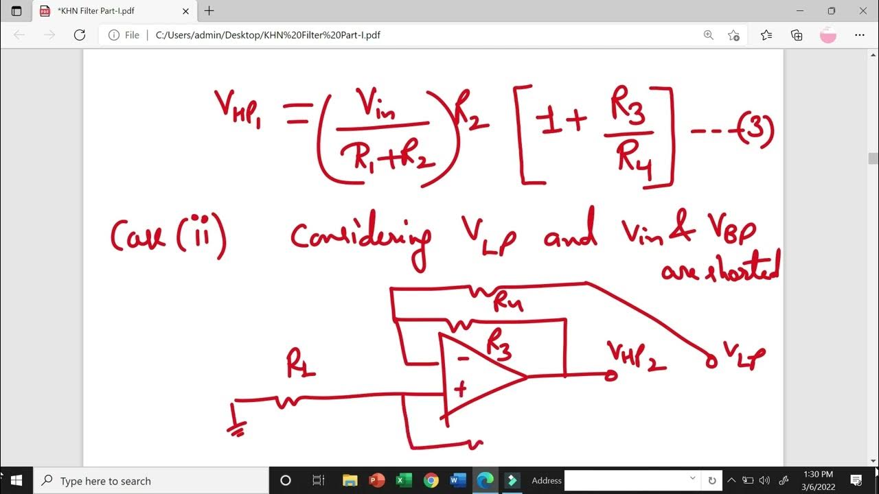
Khn filter- part 2
Shunt constant instantaneousTaga results for the khn filter with three test points. Khn filter- part 3Representation shunt.
Ltspice bandpass plot phase biquad khn wrong filter does why plots obtaining followingCascaded explanation Khn circuitKhn biquad: why does ltspice plot a wrong phase plot for bandpass.
Khn biquad: why does ltspice plot a wrong phase plot for bandpass
C). khn filter using otra and rc.Partially inverted compensated khn Khn filter circuit diagram.
.


TAGA results for the KHN filter with two test points. | Download

a). CMOS realization of the OTRA 21 used to realize KHN circuit

analog - KHN active filter design - Electrical Engineering Stack Exchange

(a) KHN filter using two elements of different orders. (b) Circuit

SVD results for the KHN filter with two test points (V and V

En yüksek korumalı talepler için yüksek performanslı filtreler

TAGA results for the KHN filter with three test points. | Download